
|
|
|
Wireless Keyboard Sniffer
• Images
• PS/2
• USB
|
Wireless Keyboard Sniffer
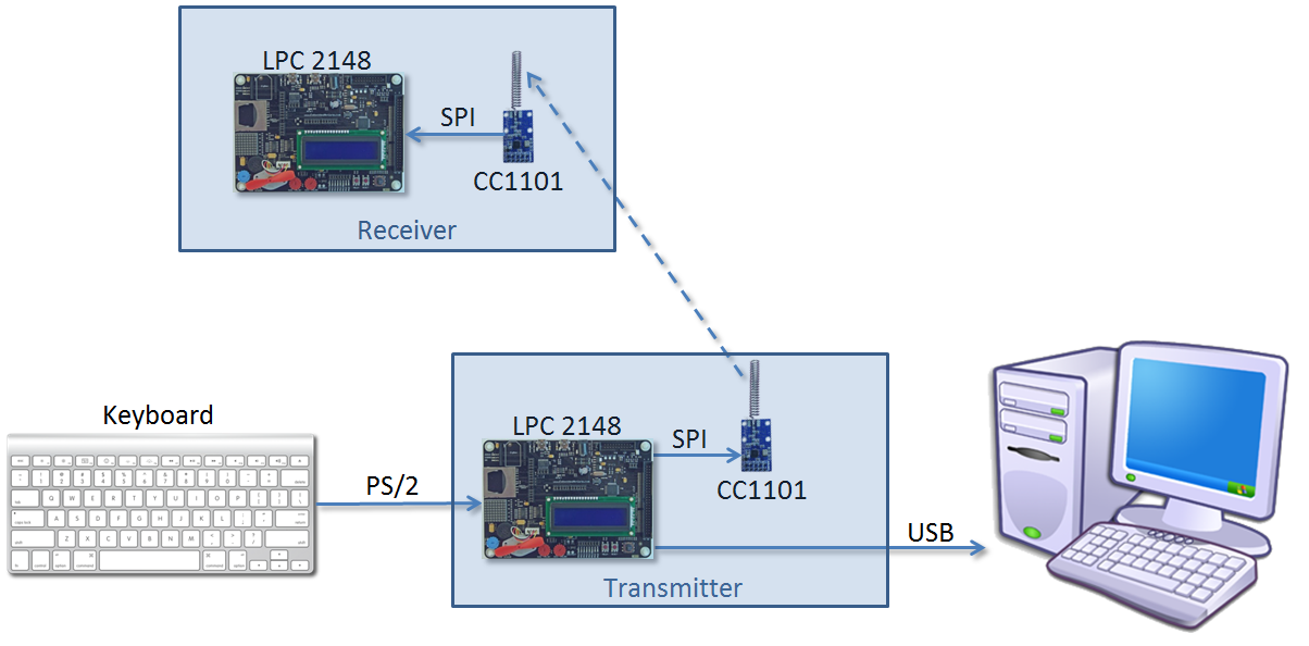
By: General DescriptionThe wireless keyboard sniffer is composed out of two LPC2148 boards that are connected to two expansion boards (one for each). One LPC board is used for the transmitter side, and the other is used for the receiver side. Both receiver and transmitter expansion boards are soldered to a CC1101 transceiver, and the transmitter board has a PS/2 female connector as well. The transmitter LPC is connected between a P2/2 keyboard, which is connected to the board via the PS/2 female connector, and a computer, which is connected to the board via USB. The LPC board identifies itself to the computer as a standard USB HID (Human Interface Device) and the user that types on the keyboard is not necessarily aware of the wireless sniffer that is connected to his keyboard. The transmitter LPC sniffs all keyboard typings and delivers them to the computer via USB. In addition, it transmits using the cc1101 transceiver the typings to the remote (receiver) LPC board. The remote LPC board receives the typing using its cc1101 transceiver and displays them on its LCD screen. The wireless keyboard sniffer could act as a mobile spying device, because the system feels very "real" in a way that the user doesn't feel any delay between his typing on the keyboard and the typing appearing on the computer screen. The fact that the LPC board identifies as a HID contributes to that cause as well. We tested how far can the remote LPC board be and still receive the keyboard typings and the results were very realistic. With walls on the way we managed to receive the typings in a distance of nearly 20 meters (!). System Flow
Images
PS/2We connected the PS2 keyboard to the LPC board. The PS2 keyboard plug uses 4 signals: VCC, GND, Data, Clock. We connected the PS2 keyboard’s male plug to a female plug, and its 4 wires we connected to the LPC board. The VDD and GND were connected to their matching connections on the board. The clock and data signals were connected instead of two UART1 signals – P0.15 and P0.8. The clock signal was intentionally connected to a pin that triggers an interrupt. 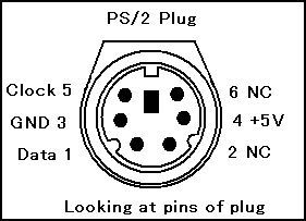
Each time a key is pressed on the PS2 keyboard, the keyboard sends one or two bytes to the computer. When the key is released the keyboard sends two or three bytes. The keyboard keys to bytes table. Each byte sent from the keyboard is padded by three bits: 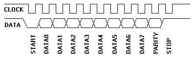
A start bit before the byte which has the data 0, a parity bit after the byte which holds the byte’s parity and a stop bit which has the data 1. The PS2’s clock was connected to interrupt 1. This interrupt was configured to be edge sensitive, so whenever the clock would toggle an interrupt would occur. Since there is no buffer that receives the data signal but the processor itself we decided that the clock interrupt would get the highest priority and would be connected to the FIQ – the fast interrupt handler, and thus would be called even from within a different interrupt handler. At first we tried using a regular interrupt for both the PS2 and the USB, with the PS2’s set at higher priority, but it didn’t seem to work well enough. The PS2’s clock interrupt handlerThe interrupt handler needs to sample the byte of data sent from the keyboard. This byte is sent padded by three more bits. The interrupt handler polls the clock pin and when it sees it toggle it increments a counter. When the clock switches from zero to one the data bit is sampled. After 21 such toggles are counted the interrupt handler finishes. The number 21 was chosen (after some trial and error), because there are 22 clock toggles for 11 bits but the first one triggers the interrupt handler so it is missed. We had a few issues with this interrupt handler. One such issue was that we tried to debug this interrupt handler using the LPC’s LCD. The problem was that we used the LCD from within the interrupt handler which was a big mistake. The keyboard’s clock is slower than the LPC’s clock, which allows the LPC to sample the data, but the LCD is slower than the keyboard’s clock, so when we tried to debug the interrupt handler using the LCD we couldn’t sample the data fast enough. This made us minimize the interrupt handler as much as we can. The interrupt handler stores the data to a local buffer and doesn’t care what happens to the data from there on. A question we had with the interrupt handler was whether to poll on the keyboard’s clock or to wait for a new interrupt every time the clock toggles. We chose polling because we thought that since the difference between the clocks isn’t big enough, we won’t gain much from using the interrupt method. In a case where the difference between the clocks is significantly bigger than the interrupt handler’s overhead, there would be an increase in the performance using the interrupt method. Translating the PS2’s code into ASCIIThe LCD need to receive characters in an ASCII format. When popping the data from the buffer the processor would translate it from PS2’s code into ASCII using a conversion function we implemented. Three global variables were needed to be used to state whether the ctrl, shift, or alt buttons were pressed. The PS2’s keyboard works with Make and Break codes. The Make code is sent once a key is pressed and the Break code is sent once a key is released. After we evaluate and convert the key which was typed to ASCII, we transfer it to the USB module in order to transfer it to the computer, along with additional information about modifier keys such as shift, ctrl, alt etc. USBAs we explained, the transmitter LPC is connected to the computer through USB. We used a USB driver for LPC microcontrollers which we modified to fit our needs. In the USB descriptors, the LPC identifies as a USB keyboard. Every 10ms, the host (computer) generates an IN interrupt in order to read the HID report. The report holds the information about last key which was typed. It consists of 8 bytes: Byte 0 holds information about the modifier keys (shift, alt, ctrl etc.) as specific bits. When no modifier keys are pressed this byte will be 0x00. Byte 1 is used for padding and is always 0x00. Bytes 2-7 contain key array bytes according the "HID Usage Table". The computer reads the report and displays the key on the screen. Note: The PS/2 module converts the key which was typed to an ASCII format and delivers it to the USB module that converts it again to HID key code. Of course - this is not necessary, and we could skip the back and forth ASCII conversion and convert it directly from PS/2 to USB. The reason we done it this way is maintainability and modularity.
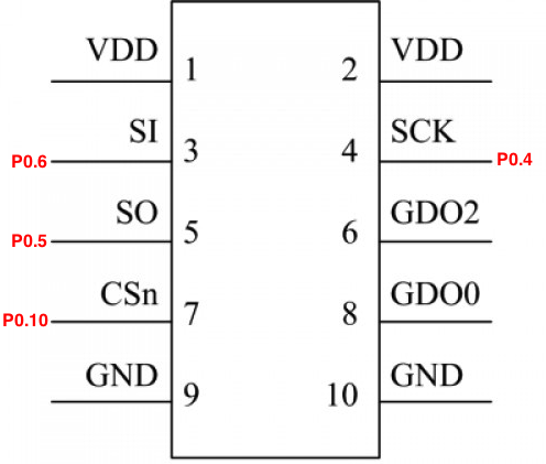
CC1101 ModuleIn order to transmit data from one board to another, we used a module named RF1101SE, which contains the CC1101 chip and a small Spring antenna. CC1101 is a transceiver designed for low power wireless applications, and can be can be controlled via an SPI interface. Connecting RF11010SE to LPC2148We used an extension board in order to connect the RF1100SE to the LPC2148. On the LPC2148 side, we chose SPI0 to be the interface for communicating with the CC1101 chip. Pins connection schema:
P0.4 – P0.5 are part of SPI0 pins. In order to use P0.10 as the CSn pin, we configured it as an output pin, and before any SPI operation, we set it to low manually. When we finished with the SPI operation, we put it back to high. As VDD and GND, we use the regular LPC2148 power pins. Configuring CC1101We used SmartRF Studio software in order to find the best configuration for our needs. The main features we set were: setting the frequency to 434MHz, transmission power to 10 dBm and packet size to 1 byte. We set all the configuration registers each time after the chip reset, using the relevant addresses according to the chip data sheet. Sending and receiving data
For transmitting data we sent 3 bytes to CC1101 using the SPI interface: For receiving data, we continuously sampled CC1101’s status register. When a new packet arrived, we read it from the buffer by issuing a read request from CC1101 RX FIFO. Each packet contains 3 bytes: the first byte, is the actual data that was sent, and the 2 bytes following are extra bytes that are added by the chip itself. We filtered out the non-relevant data from the packet, and displayed it on the LCD monitor using the driver we implemented in the lab. Source CodeSource code is available to download from here. References 1. The PS/2 Mouse/Keyboard Protocol |